Selecting custom open frame touch monitors for an AI hardware project seems like a display specification exercise — until interface mismatches, thermal conflicts, and mechanical fit problems surface weeks before production tooling. These failures are preventable, but only when the display supplier enters the design process early enough to influence decisions that matter.
For edge AI OEM/ODM projects, custom open frame touch monitors must be co-designed around three integration risks: signal interface compatibility with inference mainboards, thermal coexistence with high-heat SoCs in sealed enclosures, and structural fit with the final product housing. Solving these requires your monitor supplier to review your mainboard datasheet before PCB layout freeze — not after.
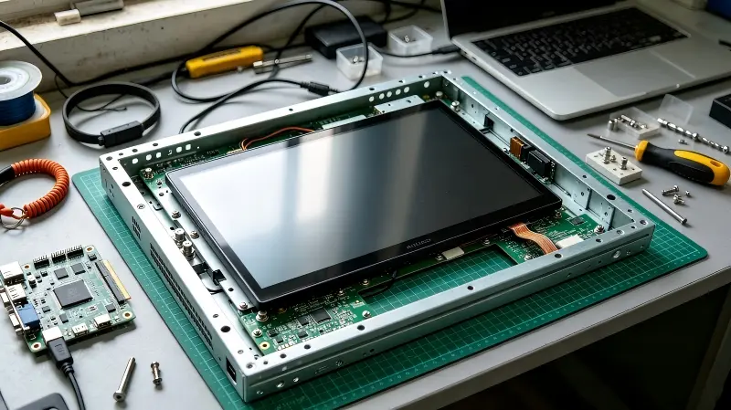
The sections below break down each integration risk in the order hardware engineers typically encounter them — and explain how early supplier engagement prevents costly rework at each stage.
If you are still choosing between ready-made and custom, the Open Frame Monitor Guide summarizes the standard LH and LD range (sizes 6.5" to 19", brightness, touch and interfaces) as the baseline your project would customize.
Why Is Interface Mismatch the #1 Hidden Risk in AI Display Integration?
Edge AI mainboards rarely output standard HDMI. Engineers who assume otherwise discover the mismatch after board layout is locked — when fixing it means redesigning the signal path or accepting an ugly adapter chain.
Most inference platforms based on Jetson, Rockchip, or Hailo architectures output eDP, LVDS, or MIPI-DSI natively. A custom open frame touch monitor for these projects needs a matched driver board that accepts the actual signal type — not a generic HDMI controller board.
How Does This Problem Appear in Real Projects?
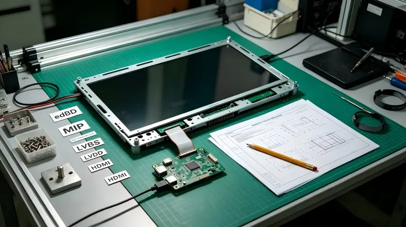
In our projects, the pattern repeats: a hardware team selects an LCD panel based on size and resolution, assumes they will connect via HDMI, then discovers their SoC only exposes eDP or a 4-lane MIPI-DSI connector[1]. At that point, three things happen:
- Adding an HDMI conversion chip increases BOM cost, board area, and power draw
- Re-routing signals requires a PCB respin — adding 4–6 weeks minimum
- Using a mismatched driver board introduces signal integrity issues at higher resolutions
What Should the Workflow Look Like?
When we review a customer's board schematic, our first step is identifying the display output signal type and available connector. From there, we recommend or design a driver board that accepts that signal directly and drives the selected panel. This eliminates conversion stages.
| Signal Type | Common AI Platforms | Driver Board Approach |
|---|---|---|
| eDP | Jetson Orin, some Rockchip[2] | Direct eDP-to-panel driver, no conversion |
| MIPI-DSI | Rockchip RK3588, MediaTek | MIPI-DSI receiver + panel timing controller |
| LVDS | Legacy or cost-optimized boards | Standard LVDS driver, widely available |
| HDMI | Only if SoC exposes it externally | Generic HDMI controller — simplest case |
The critical timing point: this decision must happen before your PCB layout freeze. Once the connector footprint and signal routing are committed, changing the display interface becomes a board respin problem.
How Does Thermal Proximity Affect Open Frame Monitors in AI Enclosures?
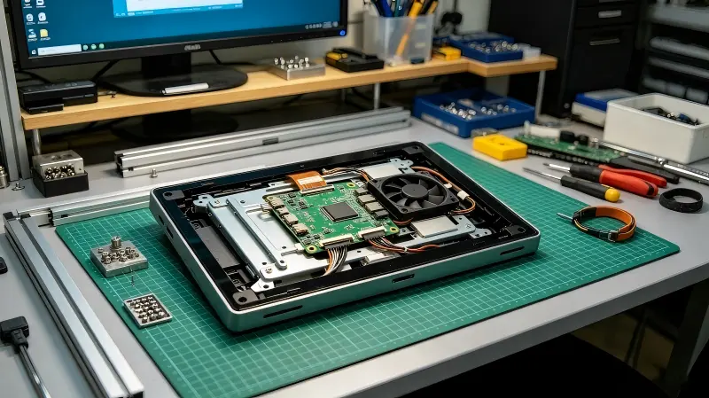
A display that passes bench testing at 25°C ambient may fail within months when mounted millimeters from an inference module dissipating 15W–75W continuously inside a sealed enclosure[3].
The "operating temperature range" on a panel datasheet is not a guarantee — it is a boundary condition. When your enclosure's internal ambient exceeds that range due to SoC heat, backlight lifetime, touch controller reliability, and LCD response all degrade[4].
Why Is This Different From Standard Industrial PC Applications?
Standard industrial PCs generate moderate, intermittent heat. Edge AI inference modules generate sustained thermal loads — often at 80–100% GPU utilization for hours or days[5]. This changes the thermal environment inside the enclosure from a manageable condition to a persistent stress factor.
What Can a Display Supplier Do About It?
We do not position ourselves as thermal engineering consultants. We do not run CFD simulations for customers. However, based on repeated OEM engagements, we address thermal risk through practical measures:
- Component selection: recommending panels and backlight LEDs rated for extended temperature ranges when the enclosure design suggests elevated ambient
- Positional planning: advising on minimum clearance between the monitor's active area and the nearest heat source[6]
- Mechanical layout: designing the open frame structure to avoid trapping hot air directly behind the panel
- Driver board placement: positioning electronics away from the thermal path of the inference module
The key takeaway: discuss your enclosure's thermal architecture with your display supplier. If your AI module sits directly behind the screen with no airflow path, that is a design constraint we need to know about during quoting — not after first article samples arrive.
Why Must Structural Customization Start Before Enclosure Tooling?
Open frame monitors exist precisely because standard enclosures do not fit custom products. But the structural flexibility that defines open frame — exposed mounting points, minimal bezel, adjustable depth — only delivers value if the monitor dimensions are co-designed with the enclosure.
Late engagement with the display supplier creates a common failure: the enclosure is already tooled, and the monitor's bezel width, mounting hole spacing, or overall depth does not match. Reworking injection mold tooling is expensive[7]. Reworking it twice is a project-killing cost.
What Dimensions Are Actually Customizable?
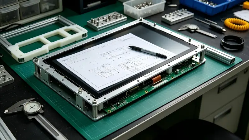
In our standard workflow for AI hardware OEM projects, we customize:
- Bezel width — often minimized to near-zero for edge-to-edge aesthetics in retail or kiosk applications
- Mounting hole pattern — matched to customer boss positions, not forced into VESA patterns
- Overall depth — critical in thin-profile devices where every millimeter behind the panel is contested space
- Cable exit direction — top, bottom, or side FPC/cable routing to match internal harness layout
- Touch sensor stack — projected capacitive with specific cover glass thickness to match flush-mount requirements[8]
When Is "Early Enough"?
The answer is: when your enclosure is still in 3D concept phase, before you commit to steel for mold tooling. At that stage, we can provide mechanical drawings, recommend mounting approaches, and confirm that the display assembly fits your volume envelope. Once tooling is cut, changes become compromises.
Frequently Asked Questions
Can you work from our mainboard datasheet to recommend a complete display solution?
Yes. Our standard process begins with your mainboard datasheet. We identify the display output signal, recommend a matching driver board, confirm panel compatibility, and deliver a structurally integrated open frame unit ready for your enclosure.
What screen sizes do you support for AI hardware OEM projects?
We supply custom open frame touch monitors from 7" to 32"+ for edge AI applications. Size selection depends on your enclosure constraints and viewing distance requirements rather than a fixed product catalog.
Do you require minimum order quantities for custom configurations?
MOQ depends on the level of customization. Driver board selection and mechanical adjustments have lower thresholds than fully custom tooling. We discuss this during initial project review.
How long does the customization process typically take from datasheet review to samples?
For projects where the signal interface and mechanical envelope are defined, first article samples typically arrive within 4–6 weeks. Complex custom tooling extends this timeline.
Conclusion
Custom open frame touch monitors for AI hardware OEM and ODM projects succeed or fail based on integration decisions — not display specs. Interface compatibility with your inference mainboard, thermal coexistence inside sealed enclosures, and structural co-design with your housing are the three risks that determine whether your product ships on schedule.
At AplusLCD, our workflow starts where these risks live: with your mainboard datasheet and your enclosure concept. If you are in the integration design phase of an edge AI product and need a display supplier who understands these constraints, share your project details with our engineering team for an initial assessment. For the full scope of what we can manufacture for you — custom sizes, brightness, touch, and interfaces, with no MOQ and CE/FCC/RoHS certification — see our custom OEM/ODM LCD display manufacturing page.
Footnotes
-
"Display Serial Interface", https://en.wikipedia.org/wiki/Display_Serial_Interface. The MIPI Display Serial Interface (DSI) specification, maintained by the MIPI Alliance, defines a high-speed serial interface supporting 1 to 4 data lanes, with 4-lane configurations commonly used in embedded and mobile SoC platforms to achieve sufficient bandwidth for HD and FHD panel resolutions. Evidence role: definition; source type: institution. Supports: MIPI-DSI supports up to 4 data lanes as defined in the MIPI Alliance specification. Scope note: Actual lane count exposed by a given SoC depends on the specific implementation and may be fewer than 4 lanes ↩
-
"NVIDIA Jetson Orin NX Series", https://developer.nvidia.com/downloads/jetson-orin-nx-series-data-sheet. The NVIDIA Jetson Orin series module datasheet and design guide list eDP 1.4a as a supported native display interface on the module connector, enabling direct panel connection without protocol conversion on appropriately designed carrier boards. Evidence role: general_support; source type: other. Supports: NVIDIA Jetson Orin modules provide eDP as a native display output interface. Scope note: Available interfaces depend on the specific Orin variant (AGX, NX, Nano) and carrier board implementation ↩
-
"Maximum power consumption bounds for Orin AGX", https://forums.developer.nvidia.com/t/maximum-power-consumption-bounds-for-orin-agx/323456. NVIDIA specifies the Jetson Orin NX at 10–25W configurable TDP and the Jetson AGX Orin at 15–60W, while high-performance edge inference accelerators can exceed 75W under sustained workloads. Evidence role: statistic; source type: other. Supports: Edge AI inference modules operate within a 15W–75W thermal design power range depending on the platform. Scope note: Actual power dissipation depends on workload, power mode configuration, and whether the module operates at peak or sustained inference loads ↩
-
"Wide Temperature TFT LCD: How to Choose the Right Displays", https://www.rocktech.com.hk/rocktech-blog/wide-temperature-tft-lcd-guide/. LED reliability studies demonstrate that backlight LED luminous flux degradation accelerates exponentially with junction temperature increases, with a commonly cited rule that every 10°C rise above rated conditions approximately halves useful lifetime; LCD panels exhibit increased response times and reduced contrast at elevated temperatures. Evidence role: mechanism; source type: research. Supports: LED backlight lifetime decreases significantly with elevated operating temperatures, and LCD optical performance degrades at high ambient temperatures. Scope note: Degradation rates are highly dependent on specific LED and LCD chemistries, and manufacturer-specific thermal ratings vary considerably ↩
-
"Timing and Memory Telemetry on GPUs for AI Governance", https://arxiv.org/html/2602.09369v1. Studies of production ML inference deployments show that dedicated inference accelerators commonly sustain 70–100% utilization during continuous operation, particularly in video analytics and real-time detection applications where frames are processed without idle intervals. Evidence role: general_support; source type: research. Supports: Production AI inference deployments at the edge sustain high GPU utilization rates for extended periods unlike intermittent desktop or industrial PC workloads. Scope note: Utilization patterns depend heavily on the specific application; batch inference or event-triggered systems may have lower sustained utilization ↩
-
"7.0 Thermal Control", https://www.nasa.gov/smallsat-institute/sst-soa/thermal-control/. Thermal design guidelines for enclosed electronics recommend maximizing physical separation between high-power dissipating components and thermally sensitive devices, as radiative and convective heat transfer intensity decreases with distance, reducing thermal coupling in confined spaces. Evidence role: general_support; source type: education. Supports: Maintaining physical clearance between heat-generating and heat-sensitive components is a standard thermal management practice in enclosed electronics. Scope note: Specific minimum clearance values depend on power levels, enclosure geometry, airflow conditions, and component thermal ratings ↩
-
"Should You Modify Your Injection Mold or Build a New Mold?", https://sybridge.com/modify-your-injection-mold-or-build-new-mold/. Industry references indicate that injection mold tooling for consumer electronics enclosures typically costs $10,000–$100,000+ depending on complexity, with engineering change modifications to existing tools ranging from $2,000–$20,000 per revision and adding 2–6 weeks to production schedules. Evidence role: general_support; source type: other. Supports: Injection mold tooling modifications are expensive, often costing thousands to tens of thousands of dollars per revision. Scope note: Costs vary widely based on mold complexity, material, geographic location of tooling vendor, and extent of required modification ↩
-
"Projected Capacitive Touch Screens - Stanford University", http://large.stanford.edu/courses/2012/ph250/lee2/. Projected capacitive (PCAP) touch technology relies on detecting changes in mutual or self-capacitance through a dielectric cover layer; increasing cover glass thickness attenuates the electric field reaching the finger, requiring touch controller sensitivity tuning, with typical consumer PCAP sensors supporting 0.5–6mm cover glass depending on controller capability. Evidence role: mechanism; source type: research. Supports: Projected capacitive touch sensors have sensitivity constraints related to cover glass thickness that affect detection reliability. Scope note: Maximum supported cover glass thickness varies by touch controller IC and sensor pattern design ↩